ICs & ChipsCode 026ee30f33
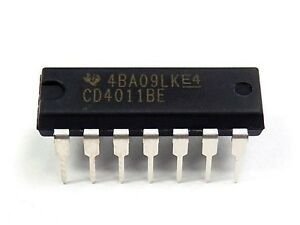
CD4011 - Quad 2-Input NAND Gate
Dual input Quad NAND gate operation .
- Delivery in 2 to 4 working daysFree in Islamabad & Rawalpindi above Rs 5,000
- Cash on deliveryPay when your parcel arrives
- 7-day checking warrantyDead-on-arrival items replaced
- Packed with careAnti-static & padded packaging
Highlights
- Dual input Quad NAND gate operation .
- Power dissipation of 100mW per logic change.
- It is available in different outline packages
- The propagation delay time is 60ns
- All input and output pins are buffered for high throughput
- The output characteristics are standardized symmetric
- CD4011 draws a maximum input current of 1 Ampere at 18 volts
- Offers different noise margin level according to the input voltage level
Specifications
- Pin number
- Pin Name
- INPUT A
- INPUT B
- LOW (0)
- LOW (0)
- HIGH (1)
- LOW (0)
- Input voltage range
- 0.5 to VDD +5V
About this product
•Temperature operating range is -55C to +125C
CD4011 - Quad 2-Input NAND Gate IC. It is a quadrable NAND gate integrated circuit that means it consists of 4 NAND gates in a single unit. It is based on CMOS logic. All inputs and outputs are designed according to the CMOS logic voltage level. It is used to execute NAND logic or you can use a combination of four gates to perform AND A= X x Y or OR B = X+Y operation also. All logical inputs and outputs of NAND. I/O pins are buffered for throughput.
Pin configuration details CD4011
This table provides details of all pins given in the above pinout.
Pin number
Pin Name
Function
1
INPUT A
Input pin first NAND gate
2
INPUT B
Input pin first NAND gate
3